Ripple carry adder
In this article, learn about Ripple carry adder by learning the circuit. A ripple carry adder is an important digital electronics concept, essential in designing digital circuits.
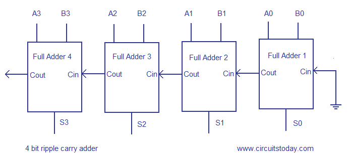
Ripple carry adder circuit.
Multiple full adder circuits can be cascaded in parallel to add an N-bit number. For an N- bit parallel adder, there must be N number of full adder circuits. A ripple carry adder is a logic circuit in which the carry-out of each full adder is the carry in of the succeeding next most significant full adder. It is called a ripple carry adder because each carry bit gets rippled into the next stage. In a ripple carry adder the sum and carry out bits of any half adder stage is not valid until the carry in of that stage occurs.Propagation delays inside the logic circuitry is the reason behind this. Propagation delay is time elapsed between the application of an input and occurance of the corresponding output. Consider a NOT gate, When the input is “0” the output will be “1” and vice versa. The time taken for the NOT gate’s output to become “0” after the application of logic “1” to the NOT gate’s input is the propagation delay here. Similarly the carry propagation delay is the time elapsed between the application of the carry in signal and the occurance of the carry out (Cout) signal. Circuit diagram of a 4-bit ripple carry adder is shown below.
 Ripple carry adder
Sum out S0 and carry out Cout of the Full Adder 1 is valid only after the propagation delay of Full Adder 1. In the same way, Sum out S3 of the Full Adder 4 is valid only after the joint propagation delays of Full Adder 1 to Full Adder 4. In simple words, the final result of the ripple carry adder is valid only after the joint propogation delays of all full adder circuits inside it.
Full adder.
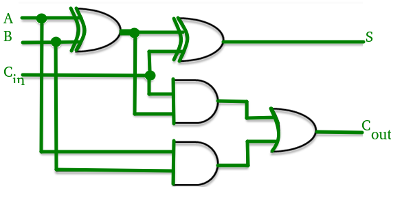
To understand the working of a ripple carry adder completely, you need to have a look at the full adder too. Full adder is a logic circuit that adds two input operand bits plus a Carry in bit and outputs a Carry out bit and a sum bit.. The Sum out (Sout) of a full adder is the XOR of input operand bits A, B and the Carry in (Cin) bit. Truth table and schematic of a 1 bit Full adder is shown below
There is a simple trick to find results of a full adder. Consider the second last row of the truth table, here the operands are 1, 1, 0 ie (A, B, Cin). Add them together ie 1+1+0 = 10 . In binary system, the number order is 0, 1, 10, 11……. and so the result of 1+1+0 is 10 just like we get 1+1+0 =2 in decimal system. 2 in the decimal system corresponds to 10 in the binary system. Swapping the result “10” will give S=0 and Cout = 1 and the second last row is justified. This can be applied to any row in the table.
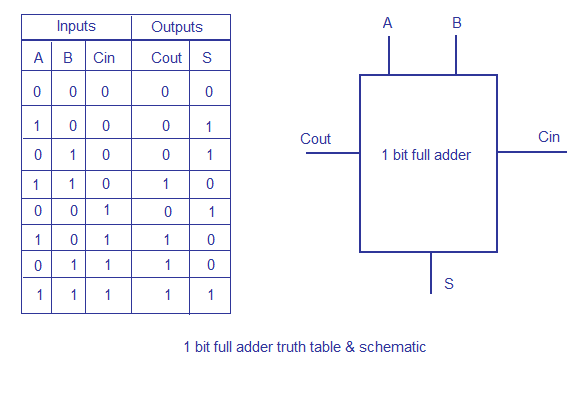 1 bit full adder schematic and truth table
A Full adder can be made by combining two half adder circuits together (a half adder is a circuit that adds two input bits and outputs a sum bit and a carry bit).
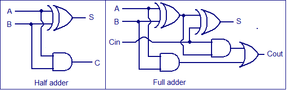 Full adder & half adder circuit
Full adder using NAND or NOR logic.
Alternatively the full adder can be made using NAND or NOR logic. These schemes are universally accepted and their circuit diagrams are shown below.
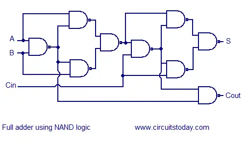 Full adder using NAND logic
 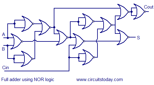 Full adder using NOR logic
Источник
What is ripple carry adder
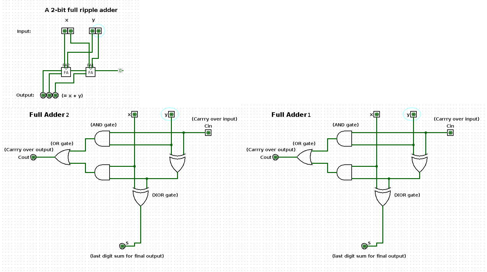
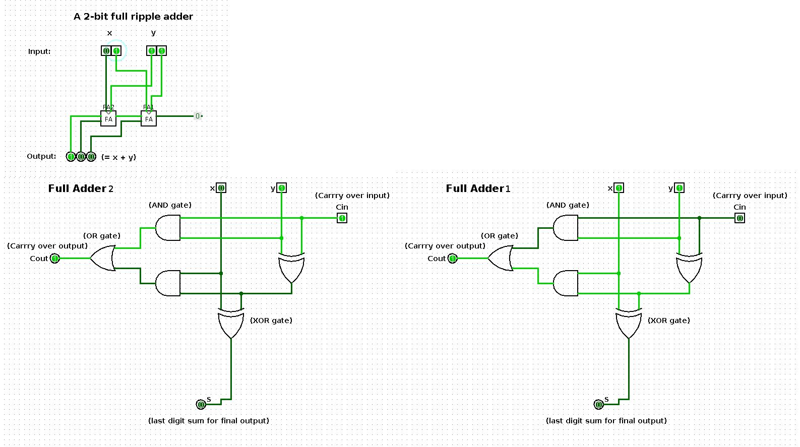
An example of how an abstract operation (addition) can be performed by a physical system.
The following shows a sequence of additions performed by a 2-bit input based ripple-carry adder (full ripple adder). Per step in the sequence one of the operands is increased by one such that the result shows a binary count from 0 up and until 100.

The two large images at the bottom represent the respective boxes in the middle of the ripple-carry adder in the top left image.
Click on the image to see it enlarged. Also see the following:
You can play with the logical circuit yourself by opening the two_bit_input_ripple_carry_adder.circ file in logisim.
What is this thing?
This ‘thing’ in the image above shows an abstract circuit for a ripple-carry adder.
A ripple-carry adder is a particular type of implementation of the component of a computer that enables it to perform addition.
The 0 and 1 signals per binary digit from x and y are physically implemented by the respective absence and presence of an electric current.
The AND, OR and XOR gates are called logical gates. These are abstractions that can be implemented in the real world using electronic components. It is useful to use abstractions because we want to be able to decouple these concepts from a specific implementation. For one because there are multiple ways these logical gates can be physically implemented.
To find out more about these logical gates and how they can be physically implemented, see here.
To get an idea how the ripple-carry adder fits into the design of a computer, see here.
States in the sequence
State 0
| x | y | x + y |
|---|---|---|
| 0 | 0 | 0 |
State 1
| x | y | x + y |
|---|---|---|
| 0 | 1 | 1 |
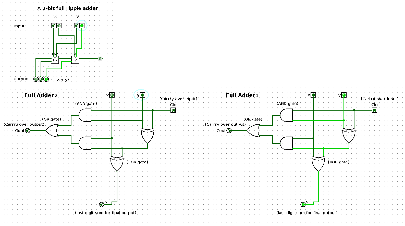
State 2
| x | y | x + y |
|---|---|---|
| 1 | 1 | 10 |
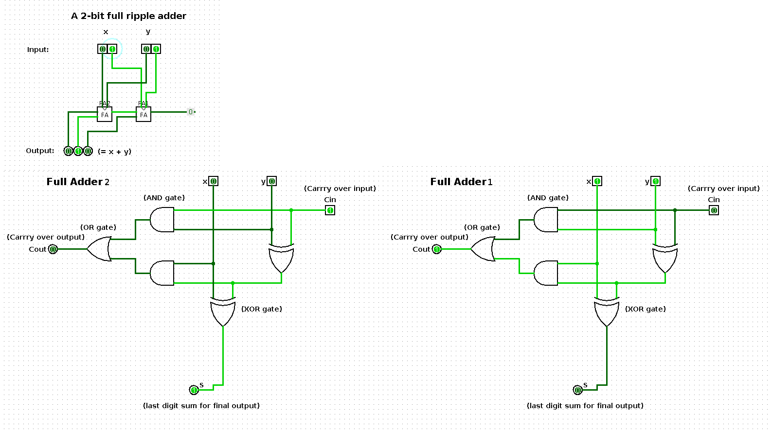
State 3
| x | y | x + y |
|---|---|---|
| 1 | 10 | 11 |

State 4
| x | y | x + y |
|---|---|---|
| 1 | 11 | 100 |
Tools used to create the sequence
- logisim (to implement logical circuits)
- shutter (to take screenshots)
- gimp (to compose shots in one image)
- convert (for gif creation)
- kazam (for video creation)
About
An example of how an abstract operation (addition) can be performed by a physical system.
Источник
What is ripple carry adder
Motivation behind Carry Look-Ahead Adder :
In ripple carry adders, for each adder block, the two bits that are to be added are available instantly. However, each adder block waits for the carry to arrive from its previous block. So, it is not possible to generate the sum and carry of any block until the input carry is known. The  block waits for the
  block to produce its carry. So there will be a considerable time delay which is carry propagation delay.
Consider the above 4-bit ripple carry adder. The sum  is produced by the corresponding full adder as soon as the input signals are applied to it. But the carry input
  is not available on its final steady state value until carry
  is available at its steady state value. Similarly depends on
  and on
  . Therefore, though the carry must propagate to all the stages in order that output and carry settle their final steady-state value.
The propagation time is equal to the propagation delay of each adder block, multiplied by the number of adder blocks in the circuit. For example, if each full adder stage has a propagation delay of 20 nanoseconds, then will reach its final correct value after 60 (20 × 3) nanoseconds. The situation gets worse, if we extend the number of stages for adding more number of bits.
Carry Look-ahead Adder :
A carry look-ahead adder reduces the propagation delay by introducing more complex hardware. In this design, the ripple carry design is suitably transformed such that the carry logic over fixed groups of bits of the adder is reduced to two-level logic. Let us discuss the design in detail.

Consider the full adder circuit shown above with corresponding truth table. We define two variables as ‘carry generate’  and ‘carry propagate’
  then,
then, 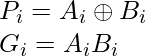
The sum output and carry output can be expressed in terms of carry generate and carry propagate as

where produces the carry when both  ,
,  are 1 regardless of the input carry. is associated with the propagation of carry from
  to
to  .
.
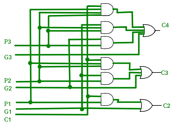
The carry output Boolean function of each stage in a 4 stage carry look-ahead adder can be expressed as

From the above Boolean equations we can observe that does not have to wait for and to propagate but actually is propagated at the same time as and . Since the Boolean expression for each carry output is the sum of products so these can be implemented with one level of AND gates followed by an OR gate.
The implementation of three Boolean functions for each carry output (, and ) for a carry look-ahead carry generator shown in below figure.
Time Complexity Analysis :
We could think of a carry look-ahead adder as made up of two “parts”
- The part that computes the carry for each bit.
- The part that adds the input bits and the carry for each bit position.
The  complexity arises from the part that generates the carry, not the circuit that adds the bits.
Now, for the generation of the  carry bit, we need to perform a AND between (n+1) inputs. The complexity of the adder comes down to how we perform this AND operation. If we have AND gates, each with a fan-in (number of inputs accepted) of k, then we can find the AND of all the bits in
  time. This is represented in asymptotic notation as
  .
.
Advantages and Disadvantages of Carry Look-Ahead Adder :
Advantages –
- The propagation delay is reduced.
- It provides the fastest addition logic.
Disadvantages –
- The Carry Look-ahead adder circuit gets complicated as the number of variables increase.
- The circuit is costlier as it involves more number of hardware.
GATE CS Corner Questions
Practicing the following questions will help you test your knowledge. All questions have been asked in GATE in previous years or in GATE Mock Tests. It is highly recommended that you practice them.
- GATE CS 2016 (Set-1), Question 43
- GATE CS 2004, Question 90
- GATE CS 2007, Question 85
- GATE CS 2006, Question 85
- GATE CS 1997, Question 15
Attention reader! Don’t stop learning now. Learn all GATE CS concepts with Free Live Classes on our youtube channel.
Источник