- Ripple carry adder
- Ripple carry adder circuit.
- Full adder.
- Full adder using NAND or NOR logic.
- Ripple Carry Adder Module in VHDL and Verilog
- VHDL Implementation:
- Verilog Implementation:
- Ripple carry adder что это
- Откройте возможности нейронного машинного перевода PROMT
- Implementation of a Simple Ternary System
- Introduction
- Ternary Logic
- Various possible representations for the ternary system
- Ternary Arithmetics
- Balanced Ternary Addition and Multiplication
- Ternary combinational circuits (Ternary gates)
- Synthesis, Minimization and Realization for Ternary Functions
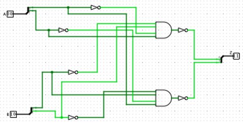
- Ternary half adder
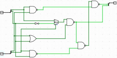
- Ternary full adder
- Ternary Full Subtractor
- Ternary Ripple Carry Adder
- Ternary Comparators
- Ternary Multiplier
- Ternary Multiplexers and Demultiplexers
- Simple Ternary D Latch
- Simple Ternary D Flip-Flap-Flop
- 1-bit Ternary Arithmetic and Logic Unit (T-ALU)
Ripple carry adder
In this article, learn about Ripple carry adder by learning the circuit. A ripple carry adder is an important digital electronics concept, essential in designing digital circuits.
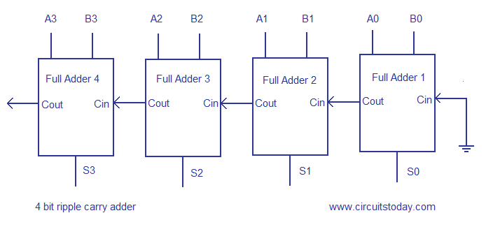
Ripple carry adder circuit.
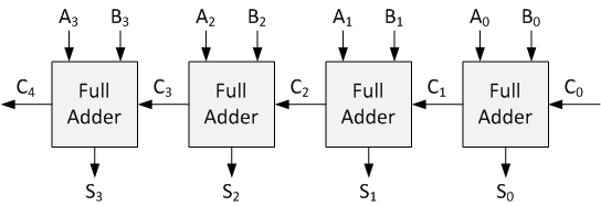
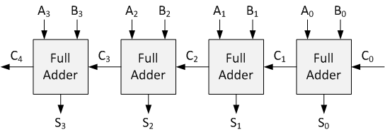
Multiple full adder circuits can be cascaded in parallel to add an N-bit number. For an N- bit parallel adder, there must be N number of full adder circuits. A ripple carry adder is a logic circuit in which the carry-out of each full adder is the carry in of the succeeding next most significant full adder. It is called a ripple carry adder because each carry bit gets rippled into the next stage. In a ripple carry adder the sum and carry out bits of any half adder stage is not valid until the carry in of that stage occurs.Propagation delays inside the logic circuitry is the reason behind this. Propagation delay is time elapsed between the application of an input and occurance of the corresponding output. Consider a NOT gate, When the input is “0” the output will be “1” and vice versa. The time taken for the NOT gate’s output to become “0” after the application of logic “1” to the NOT gate’s input is the propagation delay here. Similarly the carry propagation delay is the time elapsed between the application of the carry in signal and the occurance of the carry out (Cout) signal. Circuit diagram of a 4-bit ripple carry adder is shown below.
 Ripple carry adder
Sum out S0 and carry out Cout of the Full Adder 1 is valid only after the propagation delay of Full Adder 1. In the same way, Sum out S3 of the Full Adder 4 is valid only after the joint propagation delays of Full Adder 1 to Full Adder 4. In simple words, the final result of the ripple carry adder is valid only after the joint propogation delays of all full adder circuits inside it.
Full adder.
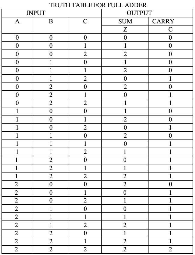
To understand the working of a ripple carry adder completely, you need to have a look at the full adder too. Full adder is a logic circuit that adds two input operand bits plus a Carry in bit and outputs a Carry out bit and a sum bit.. The Sum out (Sout) of a full adder is the XOR of input operand bits A, B and the Carry in (Cin) bit. Truth table and schematic of a 1 bit Full adder is shown below
There is a simple trick to find results of a full adder. Consider the second last row of the truth table, here the operands are 1, 1, 0 ie (A, B, Cin). Add them together ie 1+1+0 = 10 . In binary system, the number order is 0, 1, 10, 11……. and so the result of 1+1+0 is 10 just like we get 1+1+0 =2 in decimal system. 2 in the decimal system corresponds to 10 in the binary system. Swapping the result “10” will give S=0 and Cout = 1 and the second last row is justified. This can be applied to any row in the table.
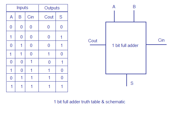 1 bit full adder schematic and truth table
A Full adder can be made by combining two half adder circuits together (a half adder is a circuit that adds two input bits and outputs a sum bit and a carry bit).
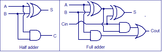 Full adder & half adder circuit
Full adder using NAND or NOR logic.
Alternatively the full adder can be made using NAND or NOR logic. These schemes are universally accepted and their circuit diagrams are shown below.
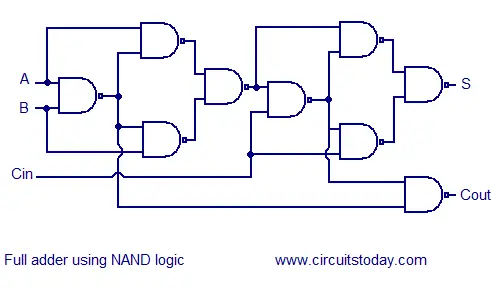 Full adder using NAND logic
 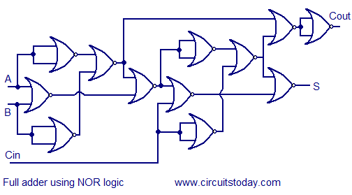 Full adder using NOR logic
Источник
Ripple Carry Adder Module in VHDL and Verilog
A Ripple Carry Adder is made of a number of full-adders cascaded together. It is used to add together two binary numbers using only simple logic gates. The figure below shows 4 full-adders connected together to produce a 4-bit ripple carry adder.
As I noted in the Full Adder tutorial, the FPGA designer doesn’t usually need to implement ripple carry adders manually. The FPGA tools are smart enough to know how to add two binary numbers together. The purpose of this exercise is to show how basic circuits can work to perform simple tasks. It is a good example for a beginner.
There are two examples in each VHDL and Verilog shown below. The first contains a simple ripple carry adder made up of just two full adders (it can add together any two-bit inputs). The second example uses a generic (in VHDL) or a parameter (in Verilog) that creates a ripple carry adder that accepts as an input parameter the WIDTH of the inputs. Therefore it is scalable for any input widths.
VHDL Implementation:
Example 1: Two-Bit Ripple Carry Adder in VHDL
Note that the ripple carry adder output (o_result) is one bit larger than both of the two adder inputs. This is because two N bit vectors added together can produce a result that is N+1 in size. For example, b»11″ + b»11″ = b»110″. In decimal, 3 + 3 = 6.
The output o_result is assigned using the ampersand (&) VHDL concatenation operator. As long as inputs to the concatenation operator of the same type they can be concatenated together.
Example 2: Scalable Ripple Carry Adder in VHDL
The second example is more complicated. The ripple carry adder below uses a VHDL generic to allow for different implementations of the same code. This makes the code more versatile and reusable. Using the generic, the code creates a generate statement which instantiates as many full-adders as are specified by the g_WIDTH generic.
This code shows how powerful generics and generate statements can be in creating code that is compact, but very scalable. It can be used for any width of inputs. The digital designer simply needs to set the g_WIDTH appropriately for his or her particular application and the tools will generate the correct amount of logic!
VHDL Testbench:
Verilog Implementation:
Example 3: Two-Bit Ripple Carry Adder in Verilog
Note that the ripple carry adder output (o_result) is one bit larger than both of the two adder inputs. This is because two N bit vectors added together can produce a result that is N+1 in size. For example, b»11″ + b»11″ = b»110″. In decimal, 3 + 3 = 6.
The output o_result is assigned using the brackets <, >Verilog concatenation operator.
Example 4: Parameterizable Ripple Carry Adder in Verilog
Again, this version of the code is more complicated. The above ripple carry adder uses a Verilog parameter to allow for different implementations of the same code. This makes the code more versatile and reusable. Using the parameter, the code creates a generate statement which instantiates as many full-adders as are specified by the WIDTH parameter.
This code shows how powerful parameters and generate statements can be in creating code that is compact, but very malleable. It can be used for any width of inputs. The digital designer simply needs to set the WIDTH appropriately for his or her particular application and the tools will generate the correct amount of logic!
Verilog Testbench:
Help Me Make Great Content! Support me on Patreon! Buy a Go Board!
Источник
Ripple carry adder что это


Откройте возможности нейронного машинного перевода PROMT
PROMT.One (www.translate.ru) – бесплатный онлайн-переводчик на основе нейронных сетей (NMT) для азербайджанского, английского, арабского, греческого, иврита, испанского, итальянского, казахского, китайского, корейского, немецкого, португальского, русского, татарского, турецкого, туркменского, узбекского, украинского, финского, французского, эстонского и японского языков.
Смотрите перевод слов и устойчивых выражений, транскрипцию и произношение в Словаре. Изучайте времена и формы глаголов в английском, немецком, испанском, французском и русском языках в разделе Спряжение и склонение. Учите употребление слов и выражений в разных Контекстах. Мы собрали для вас миллионы примеров перевода на разные языки, которые помогут вам в изучении иностранных языков и подготовке домашних заданий.
Переводите в любом месте и в любое время с помощью мобильного переводчика PROMT.One для iOS и Android. Попробуйте голосовой и фотоперевод, скачайте языковые пакеты для офлайн-перевода.
Поделиться переводом
Ваш текст переведен частично.
Вы можете переводить не более 999 символов за один раз.
Войдите или зарегистрируйтесь бесплатно на PROMT.One и переводите еще больше!

Добавить в избранное
Для добавления в Избранное необходимо авторизоваться
Источник
Implementation of a Simple Ternary System
List of accomplishments
- Basic ternary logic gates: T_NOT, T_OR, T_AND, T_NAND, T_NOR, T_XOR and more
- Synthesis, Minimization and Realization for Ternary Functions
- Ternary half adder, Ternary full adder, Ternary ripple carry adder
- Ternary full subtractor, comparator, multiplier, multiplexer/demultiplexer
- Ternary flip flap flops and latches
- A primitive Ternary Arithmetic and Logical Unit (ALU)
Conventions and used technologies
- Unbalanced Ternary (0, 1, 2) was used in implementation
- 1 Trit is expressed by 2 Bits: 0
10 (11 is undefined)
Introduction
As first-year students of Innopolis University, we had the opportunity to realize projects throughout our computer architecture course. Our group was particularly interested in the ternary system and its functioning, so we decided to implement a simple ternary system with basic components (gates).
In logic, a three-valued logic (also trinary logic, trivalent, ternary) is one of several many-valued logic systems in which there are three truth values indicating true, false and some indeterminate third value.
Ternary logic is MVL (Multi-valued logic) compliant. However, only three logic states are used, ‘0‘,’1‘ and ‘2‘. The optimum radix (r) of a fractional number is found to be the natural logarithm (e). Ternary logic uses number representation with r=3, compared to binary logic which uses r=2, hence the most economical integer radix which is the closest to the natural logarithm e, is base 3. This special property of base 3 inspired the early computer designers to build a ternary computer.
The first working ternary computer was built in Russia at the Moscow State University in 1958. The computer was designed by Nikolay Brusentsov and his colleagues. They named it Setun, like the river that flows near the university campus.
Ternary Logic
A ternary logic function is a mapping F: <0,1,2>n -> . We will discuss the advantages and disadvantages of ternary logic over binary logic.
Where Boolean logic has 2 2 = 4 unary operators, the addition of a third value in ternary logic leads to a total of 3 3 = 27 distinct operators on a single input value. Similarly, where Boolean logic has 2 2 2 = 16 distinct binary operators (operators with 2 inputs), ternary logic has 3 3 2 = 19,683 such operators. Where we can easily name a significant fraction of the Boolean operators (not, and, or, nand, nor, exclusive or, equivalence, implication), it is unreasonable to attempt to name all but a small fraction of the possible ternary operators.
Advantages of Ternary Logic
A ternary logic representation enables a more compact and efficient information encoding than the equivalent binary logic representation. The argument stated is as follows: if we assume that a digital circuit has N possible input combinations, then a binary circuit requires log2N input lines and a ternary circuit requires log3N input lines.

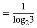

Therefore, a ternary encoded realization of a given binary logic function should require 0.63 times the input lines than the corresponding binary realization.
Disadvantages of Ternary Logic
Although ternary logic circuits should require fewer input lines than the equivalent binary logic circuits, ternary logic circuits are currently not a practical choice. The reasons are
- Ternary hardware implementation technology is still in the theoretical, simulation, and laboratory test levels
- Representing three ternary logic levels (0, 1, and 2) using voltage levels of existing technology is not yet effectively defined
- No computational model and programming language is developed. However, simulating results of ternary circuit implementation using complementary metal oxide semiconductor (CMOS), resonant tunneling diode (RTD), and carbon nano-tube technologies, demonstrating that ternary logic may be a choice for future computing.
Various possible representations for the ternary system
More about the balanced Ternary Numbering System
Today, mostly all hardware is designed for binary computing. If we had a stable electronic component with three stable states, the world perhaps would have turned to ternary computing. However, this is not the truth today. The balanced ternary radix notation has some beneficial properties:
- Ternary inversion is easy, just exchange −1 with 1 and vice versa. If we use an example, 24 is represented as 1T0, and -24 as T10 in balanced ternary notation (T is simply a notation for -1). This is simpler than the rule for the two’s complement in binary logic.
- The sign of a number is given by its most significant nonzero ’trit’
- The operation of rounding to the nearest integer is identical to truncation.
- Addition and subtraction are essentially the same operation (I.e. you merely add the digits using the rules for addition of digits)
Ternary Arithmetics
Ternary arithmetic can offer a more compact notation than binary arithmetic, and would have been an obvious choice if the hardware manufacturers would have found a ternary switch.
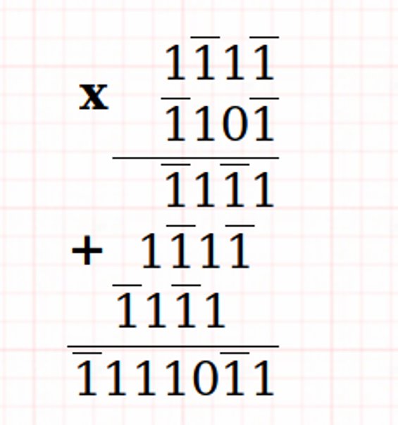
Balanced Ternary Addition and Multiplication
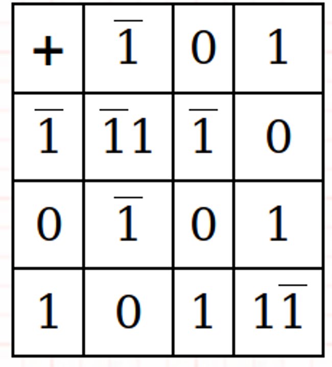
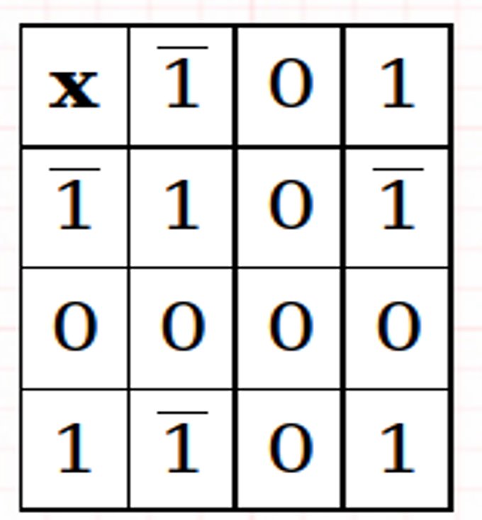
Examples: 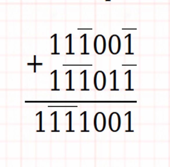
Ternary combinational circuits (Ternary gates)
A combinational circuit consists of input variables, ternary logic gates and output variables. The output of the circuit depends only upon the present input. Logic gates accept signals from the input variables and generate output signals. This process transforms ternary information from
the given input data to the required ternary output data.
As mentioned above we can easily name a significant fraction of the Boolean operators (not, and, or, nand, nor, exclusive or, equivalence, implication), however, it is unreasonable to attempt to name all but a small fraction of the possible ternary operators. We will consider the following ternary circuits:
And (Min): It is natural to extend the Boolean and function to a ternary function by declaring that the result is true only if both inputs are true, false if any input is false, and unknown otherwise.
Or (Max): It is also natural to extend the Boolean or function to ternary by declaring that the result is true if any input is true, false only if both inputs are false, and unknown otherwise.
Consensus: In Boolean logic, the inverse of exclusive or is true when the two inputs are the same, and false when they are different. There are several natural extensions of this idea to ternary logic. One of them is the logical consensus of a set of variables, which is true if all are true, false if all are false, and otherwise unknown
Any: Where consensus requires that both inputs agree before it asserts anything but unknown, the accept anything operator declares an unknown conclusion only if both inputs are unknown or actively disagree. Otherwise, it jumps to a conclusion from any non-unknown input available to it.
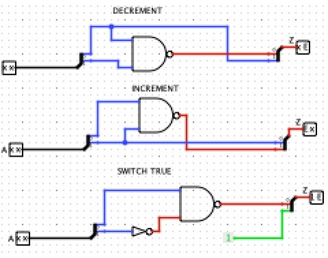
Increment and Decrement: In Boolean logic, the inverter may be thought of as incrementing or decrementing its argument modulo 2. In ternary logic, the modulo 3 increment and decrement functions are quite distinct from inversion.
Synthesis, Minimization and Realization for Ternary Functions
Relationships interrelated in the ternary logic system
A ternary logic function can be represented as a Max-Min expression. Ternary Max-Min expressions are defined as follows:
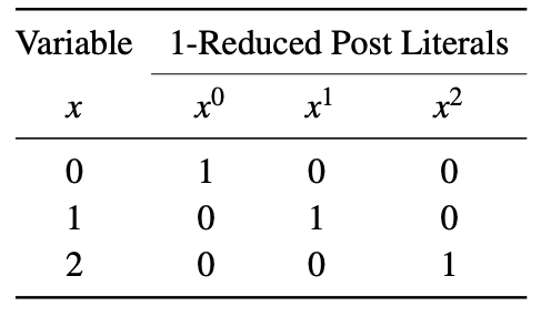
Variable: Any symbol that takes value from the set T ∈ <0,1,2>is a ternary variable.
Literal: Literals are transformed forms of a variable. They are used to form Max-Min expressions.
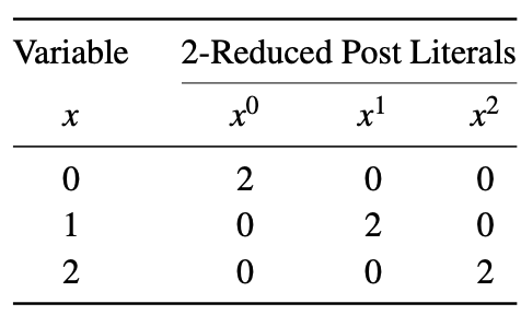
In the literature two types of literals are commonly used: 1-reduced Post literals and 2-reduced post literals. A 1-reduced Post literal of a variable x is represented as xi, where i ∈ <0,1,2>. When x = i, then xi = 1, otherwise xi = 0. The 1-reduced Post literals of a variable is shown below.
A 2-reduced Post literal of a variable x is represented as xi, where i ∈ <0,1,2>. When x = i, then xi = 2, otherwise xi = 0. The 2-reduced Post literals of a variable is shown below. This example makes use of different sets of literals to form Max-Min expressions as discussed previously.
Minterm: When literals of variables of a function are combined using the Min operation, then the term is called a minterm. For example, for a 3-variable ternary logic function F(x,y,z), xyz and xz are two examples of minterms.
Max-Min Expression: When two or more minterms are combined using Max operations, then the expression is called a Max of minterms (Max-Min) expression. For example, for a 3-variable ternary logic function F(x,y,z) = xy + yz + xyz is an example of a Max-Min expression.
Any function F(x,y,z) can always be represented as
Three basic methods to minimize ternary functions are:
- Manipulation of algebra expression as in Boolean algebra.
- The tabular method.
- Ternary K. map method.
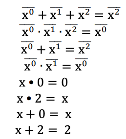
For the implementation of ternary circuits it is necessary to convert ternary variable into unary variable (using the 2-Reduced Post Literals table).
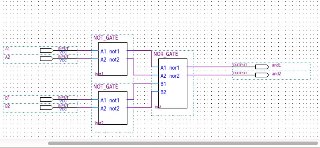
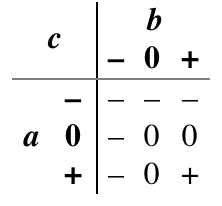
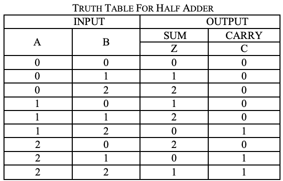
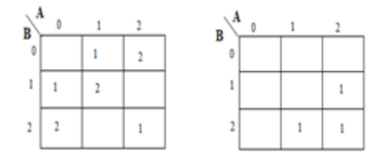
Ternary half adder
A circuit for the addition two 1 trit numbers is referred to as a half adder. the circuit does not consider a carry generated in the previous addition. The addition process in ternary logic system is shown below. Here A and B are two inputs and sum(S) and carry (CARRY)
are two outputs.
Analysis
A karnaugh map (K-map) is used to represent the sum and carry output. K-maps are useful for minimization and optimization of logic circuits. Here a K-map of 2 inputs is used. Since no grouping of 2’s and 1’is possible, the output equation is as below.
Implementation
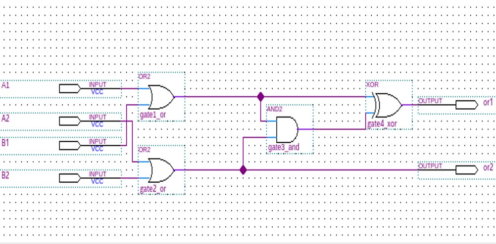
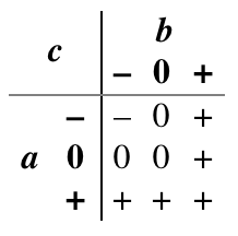
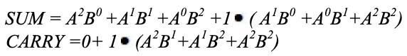
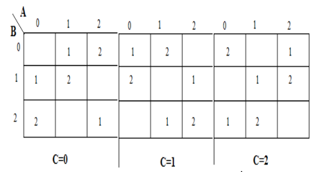
Ternary full adder
As with half adders, one stage of a ternary full adder can be described by a numerical table giving the sum SUM and carry out CARRY as a function of the three inputs A, B, along with the carry in C:
Analysis
A karnaugh map (K-map) is used to represent the sum and carry output. K-maps are useful for minimization and optimization of logic circuits. Here a K-map of 3 inputs is used.
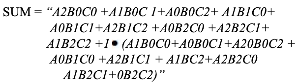
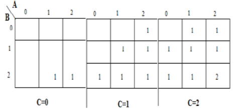
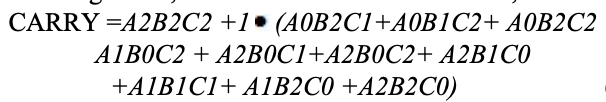
Implementation
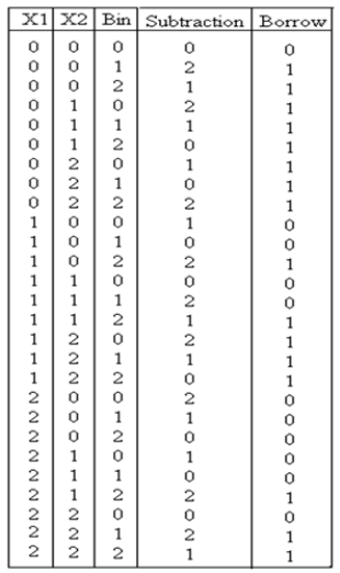
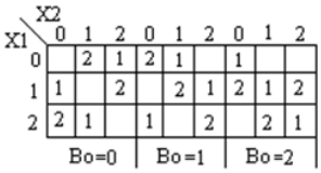
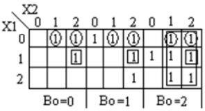
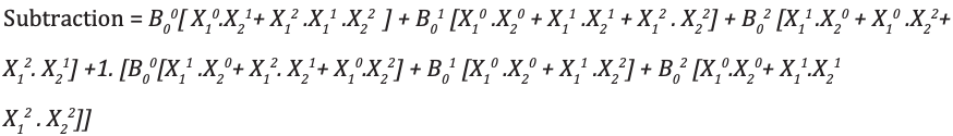
Ternary Full Subtractor
Ternary full-Subtractor is a circuit that subtracts two inputs and previous borrow. Truth table for Subtractor is shown below

Ternary Ripple Carry Adder
Ripple-carry adder(RCA) is a well-known circuit for performing addition of two numbers by cascading ternary full adders. A Ternary RCA is quite similar to its Binary counterpart. A Ternary Half Adder is employed to add the least significant Ternary digits. The rest are summed up by Ternary Full Adders. As mentioned before, Ternary Full Adder adds three Ternary input variables.
Implementation
Ternary Comparators
Ternary comparator circuit camper two inputs X1, X2 and accordingly generates output as X1 = X2, X1 > X2, X1 Analysis and Implementation
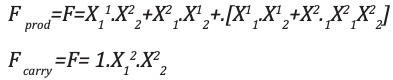
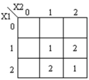
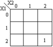
Ternary Multiplier
Ternary multiplier is a circuit that multiplies two input numbers and generates corresponding product. Truth table for this circuit is shown below:
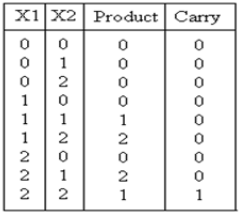
The resulting expression for the product and carry are shown:
The corresponding K-maps are shown:
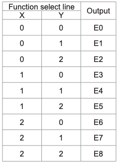
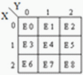
Ternary Multiplexers and Demultiplexers
Multiplexer is a circuit having multiple inputs and a single output. It is also known as decoder. The output function of the multiplexer is determined by the number of function lines. Thus for 2 trit
multiplexer the output will be 3 2 = 9 and two will be the function select lines. Multiplexer i.e. function
selection logic selects 1 out of 9 functions as an output. Function select logic is implemented using logic gates. The output equation of function selection logic is:

Demultiplexer is also referred to as encoder. Its functionality is reverse to that of multiplexer. It accepts the single input and distributes it over several outputs
Simple Ternary D Latch
Although design of circuits implementing combinational ternary logic is straightforward, the design of a simple and robust ternary memory element (i.e latch) suitable for integrated circuit (IC) implementation has been challenging. However, a simple ternary latch can be obtained by replacing the binary NOR or NAND gates used with corresponding ternary T_NOR or T_NAND gates.
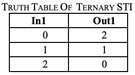
Simple Ternary D Flip-Flap-Flop
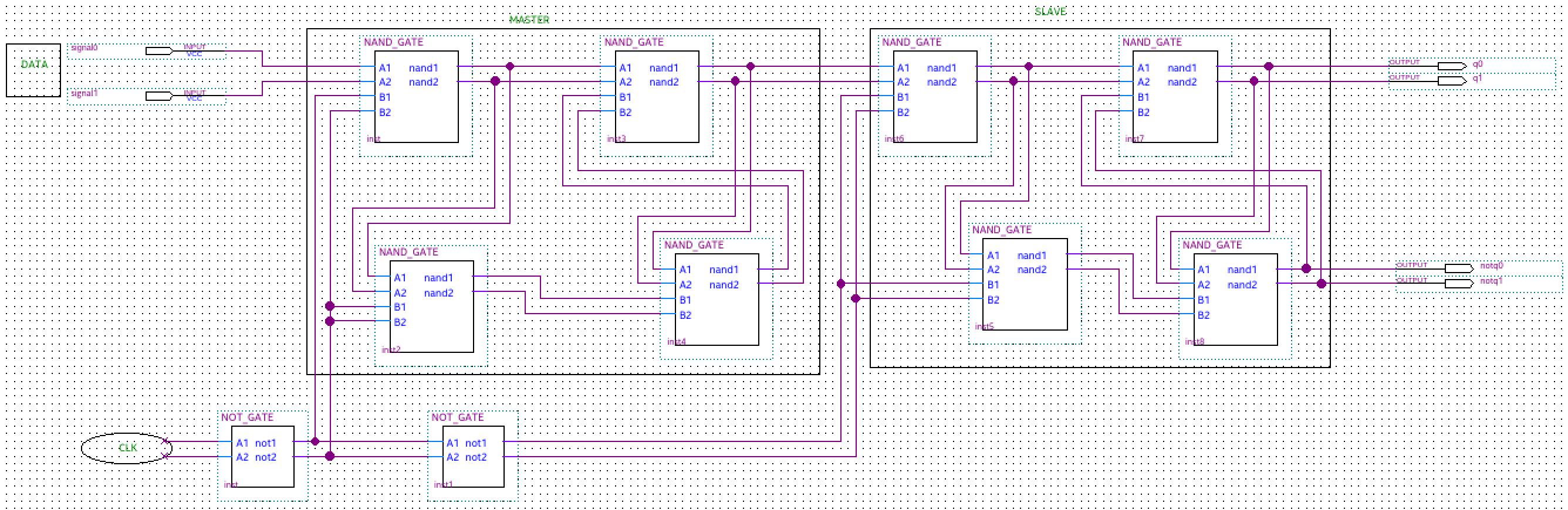
The Master Slave (MS) ternary D Flip-Flap-Flop (FFF) is realized based on the ternary D latches. This is similar to the way the binary D Flip-Flop (FF) is realized using binary D latches. The logic diagram and the operation description of the MS binary D flip-flop are well known. In order to implement the MS ternary D FFF , we replace the binary D latches with ternary D latches (realized with ternary negated-minimun gates of two inputs – NAND) and the binary inverters with simple ternary inverters (STI). The truth tables for both the ternary NAND circuits and ternary STI circuits are shown

For MS ternary D FFF with binary clock, the data are ternary (0, 1 and 2 logic) and the clock is binary (low and high – in our
implementation, 0 and 2 logic). The MS ternary D FFF with
binary clock can read the data when the clock goes from low to
high (positive edge) or from high to low (negative edge), depending
on the number of STIs.
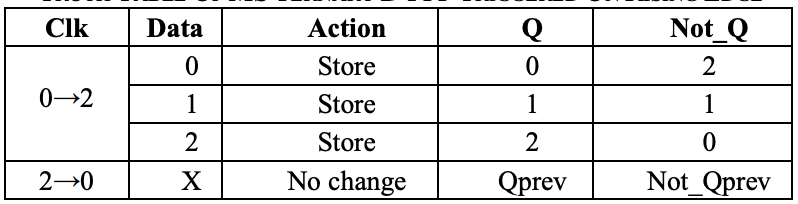
The inputs of the ternary D FFF are Data and Clk, and the outputs are Q and Not_Q. The clock signal is binary and the logic levels are denoted 0 and 2, in order to maintain the correspondence with electrical implementation

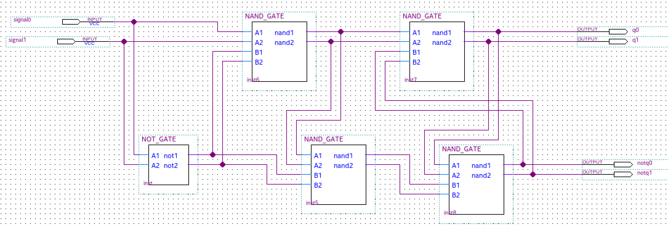
1-bit Ternary Arithmetic and Logic Unit (T-ALU)
Ternary Arithmetic Logic Unit (ALU) is a digital circuit used to perform arithmetic and logic operations. It represents the fundamental building block of the Central Processing Unit (CPU) of a ternary computer. ALU carries out arithmetic operations like addition, subtraction, multiplication, and logic operations compare, NAND, NOR, NOT, AND, and OR. Below is shown a primitive architecture of a 1 trit ALU
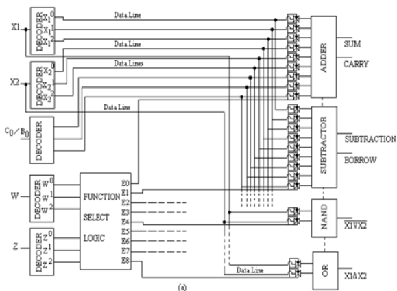
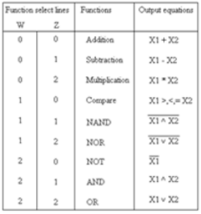

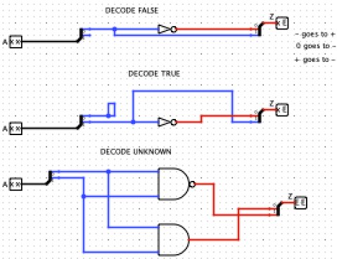
Basic building blocks of ALU are decoders, function select logic (Multiplexer), transmission gate and separate processing modules. Function selection logic selects 1 out of 9 functions listed depending upon the logic state on function select lines W and Z.
Output lines of selection logic are connected to TG (Ternary gate) associated with each module. Any module is selected only when associated TG is enabled else it is isolated from data lines. For e.g. If input from select lines W and Z = 0, output E0 of selection logic is high (2) while E1, to E8 is low (0) so, TG associated with adder module will be enable allowing data
lines to be connected to adder modules while other modules are isolated from the data lines.
Finally, by cascading n/2 trit ALU slices, an n trit ALU can be formed.
Источник